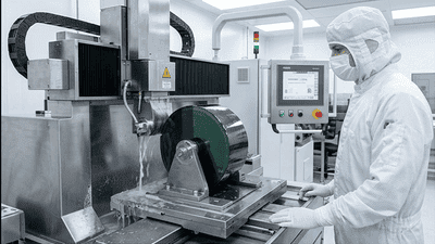
SiC Substrate Cost Curve: Approaching Silicon Parity in 2026
2026-11-09

A silicon wafer is often described as the foundation of a semiconductor. In silicon-on-insulator technology, that foundation does more than support the manufacturing process. Its engineered structure helps determine how electrical signals behave, how neighboring circuits interact, and how different functions can share a chip.
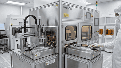
That makes SOI a distinctive opportunity within semiconductor materials. Demand is connected not only to the number of chips manufactured, but also to the value of electrical isolation in specific applications. Radio-frequency devices and smart power circuits are two important examples.
However, the opportunity needs careful boundaries. RF-SOI is not interchangeable with power-SOI, and power-SOI is not a substitute for every silicon-carbide or gallium-nitride power device. The investment case becomes stronger when those differences are understood rather than hidden beneath a broad specialty-wafer label.
A conventional bulk silicon wafer provides a continuous silicon substrate. An SOI wafer introduces an insulating layer beneath the silicon in which devices are fabricated.
In common silicon-based structures, that insulating layer is a buried oxide. The substrate therefore becomes an engineered stack rather than simply a polished silicon disc.
The arrangement changes electrical coupling and parasitic behavior. STMicroelectronics describes the buried oxide as a means of reducing parasitic capacitance in its FD-SOI technology.
For materials suppliers, the commercial product includes controlled layer properties, interfaces, geometry, and consistency. Its value cannot be judged from silicon purity alone.
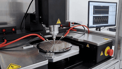
SOI encompasses multiple substrate and process configurations. RF-SOI is optimized for radio-frequency applications. Power-SOI supports selected power-management and mixed-voltage circuits. FD-SOI addresses another set of transistor and low-power design requirements.
The thickness and electrical characteristics appropriate for one application may not suit another.
This distinction matters commercially. A supplier’s total SOI capacity does not automatically translate into usable capacity for every customer or product platform.
From the procurement desk, the relevant question is whether the specific substrate is qualified for the intended process. From the investment desk, it is which qualified product family generates revenue and where its demand originates.
A wireless device must connect antennas with transmission and reception paths across different operating conditions. Switches, tuners, amplifiers, and other components help manage those functions.
RF-SOI has an established role in switches and related front-end applications. Its isolation characteristics can support the demanding combination of signal performance, integration, and manufacturing economics that these circuits require.
STMicroelectronics offers RF-SOI processes for front-end modules, including devices optimized for switches and low-noise amplifiers. Its portfolio also includes configurations supporting selected power-amplifier functions.
That does not mean an entire RF module uses one substrate technology. Different components can still rely on different materials and manufacturing processes.
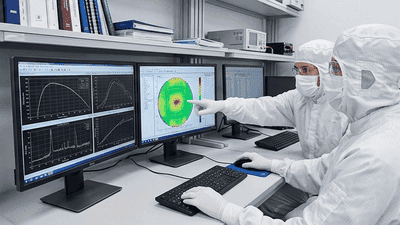
Wireless complexity can increase the need for routing, tuning, and integration. But the relationship between connectivity features and wafer demand is not fixed.
Device designers can integrate more functions, change architectures, reduce die size, or improve manufacturing yield. Those developments affect the substrate area required per finished product.
End-device volumes also matter. Greater RF content in a handset can coexist with weak handset shipments.
An investor should therefore separate three drivers: the number of devices sold, the semiconductor content per device, and the wafer area needed to manufacture that content. Combining them into one growth assumption invites disappointment.
An RF substrate must do more than provide mechanical support. Electrical behavior within the substrate and near its interfaces can affect signal losses and unwanted coupling.
RF-SOI platforms are consequently engineered around RF-specific requirements rather than adapted casually from a generic wafer.
Soitec describes its RF-SOI substrates in terms of linearity, frequency performance, power consumption, and integration benefits relative to bulk-silicon implementations. Those are application-dependent product claims, not guarantees for every circuit built on SOI.
The competitive advantage lies in delivering the substrate behavior a qualified process needs, consistently enough that designers and manufacturers can rely on it.

Power-SOI becomes especially interesting when a chip must combine control circuitry with higher-voltage functions.
A smart power device may need to manage switching, sensing, protection, communication, and diagnostic functions together. Isolation helps designers separate blocks that operate under different electrical conditions.
Soitec’s power-SOI platforms target automotive and industrial applications, including motor drivers and power-management circuits. Its product descriptions emphasize integration of high- and low-voltage functions using SOI and deep trench isolation.
The opportunity is therefore not simply “more power.” It is the ability to integrate useful intelligence around power handling while meeting application-specific robustness requirements.
Silicon carbide and gallium nitride attract attention in power electronics, but their investment narratives should not be copied directly onto power-SOI.
Power-SOI primarily describes an engineered silicon platform used in selected integrated circuits. SiC and GaN are different semiconductor materials with different device opportunities.
A system can contain several of these technologies because they perform different functions. A power stage, controller, driver, and sensing circuit need not share one material platform.
For forecasting, distinguish the market for intelligent power ICs from the market for discrete high-power switching devices. Their growth can be related without producing identical substrate demand.
Vehicles increasingly depend on electronic control, sensing, and power management. That creates opportunities for substrates supporting robust mixed-voltage integration.
Power-SOI suppliers point to applications associated with electric vehicles, driver-assistance systems, and 48-volt architectures. These are potential adoption pathways rather than a guarantee that every related chip uses SOI.
Commercial progress also depends on process qualification, customer design decisions, and production schedules.
For the supplier, an automotive design win can support a durable relationship. For the investor, it requires patience: engineering acceptance, vehicle-program adoption, and meaningful wafer purchasing are separate milestones.
Motor control, automation, and other industrial systems also combine electrical power with sensitive control functions. Suitable isolation can help manage interaction between those functions.
However, industrial markets contain many applications with different specifications and replacement cycles. There is no single industrial-SOI growth rate that captures them all.
Soitec’s power-SOI offering explicitly includes industrial applications and emphasizes noise immunity and mixed-voltage integration.
A disciplined demand model identifies the relevant IC categories, their substrate choices, and their adoption rates. Broad industrial spending is useful context, but it is not a substitute for that application map.
An engineered substrate carries additional manufacturing and quality-control requirements. The customer is paying for a structure that enables a particular process, not simply for more silicon.
Layer properties, defect control, interfaces, and lot consistency all contribute to the product’s value.
The keyword is repeatability. A wafer that performs well once is interesting; a wafer platform that performs consistently across production lots is commercially useful.
That creates room for differentiation, but a selling-price premium does not automatically produce a margin premium. More complex manufacturing can bring higher processing costs, yield challenges, and capital requirements.
Changing a substrate can affect several downstream manufacturing steps. Customers therefore have reasons to evaluate alternatives carefully before introducing them into production.
Once a wafer platform is qualified, replacing it may require engineering effort and additional testing. That supports supplier retention.
However, qualification does not make customers permanently captive. They can develop second sources, adopt new process platforms, or redesign products when the benefits justify the work.
The strongest moat combines technical capability with reliable delivery and continuing product development. Historical qualification helps, but each new application creates another competitive test.
A specialty-wafer supplier may serve a limited number of major manufacturing customers. Those relationships can provide scale, but they also create exposure to purchasing decisions and inventory changes.
A customer’s production slowdown can influence shipments even when the substrate remains technically preferred.
The supplier may also depend indirectly on a concentrated set of end markets, such as mobile devices or automotive electronics.
Investors should look beyond the number of customer accounts. Several customers can still share the same demand cycle, creating more correlated exposure than the headline diversification suggests.
Moving a process to a larger wafer diameter can affect output and cost, but it requires compatible manufacturing infrastructure and a successful process transition.
For substrate suppliers, the transition changes the product and capacity mix. Wafer counts alone become less informative when diameters differ.
In June 2026, Soitec and ZenSemi announced a collaboration supporting a 300-millimeter BCD-on-SOI process using power-SOI substrates. The announcement described development and capacity ramp-up, not completed proof of commercial volume.
That distinction matters: a larger-diameter platform can create opportunity well before it produces substantial recurring revenue.
Specialty does not mean noncyclical. Wafer customers can accumulate inventory, reduce purchasing, and later replenish stock.
Supplier shipments may consequently diverge from actual device demand. During destocking, customers can continue production while buying fewer substrates.
When replenishment begins, shipments can improve faster than underlying consumption.
The analyst should reconcile substrate sales with customer inventories, fabrication activity, and end-market conditions. Otherwise, a temporary purchasing adjustment may be mistaken for either structural decline or an unusually strong new growth phase.
Capacity announcements often attract attention, but nameplate output is not the same as customer-accepted production.
New equipment, facilities, or manufacturing routes need consistent results and appropriate customer approval. Different SOI platforms may also impose different processing requirements.
A useful capacity assessment separates installed capacity, demonstrated productive output, qualified capacity, and actual shipments.
Supply resilience benefits from multiple dependable production routes. Yet establishing those routes requires investment and disciplined execution, not merely announcing geographic diversification.
SOI does not replace photoresists, process gases, targets, or cleaning chemicals. Devices built on engineered wafers still require extensive downstream manufacturing.
Changes in substrate technology can alter process requirements and create opportunities for related materials suppliers.
But those opportunities must be identified individually. A qualified SOI process does not imply that every consumables category experiences the same increase in value or volume.
For portfolio construction, separate direct substrate exposure from broader materials participation. The connection is real at the manufacturing level, but the financial sensitivity can differ substantially.
Assess the opportunity through specific operating questions:
These questions connect the technical differentiation with the economics shareholders actually receive.
SOI’s appeal comes from making the substrate an active contributor to device performance. In RF, that supports selected switching, amplification, and integration requirements. In smart power, it supports selected mixed-voltage and control applications.
The specialty-wafer opportunity is therefore more precise than a general bet on semiconductor growth. It depends on where isolation delivers enough system value to justify an engineered substrate.
Companies that translate that value into qualified production, reliable supply, and sound returns can build durable positions. Investors who distinguish product platforms, adoption milestones, and inventory effects will be better placed to recognize them without overstating the addressable market.