High-Purity Quartz Supply Risk: The Monocrystal Pulling Bottleneck
2026-10-29

The wiring inside a semiconductor is becoming as important to performance as the transistors it connects. As features shrink, moving electrical signals through narrow lines and tiny connections becomes increasingly difficult. Resistance, reliability, and manufacturing consistency turn metallization into a materials-engineering challenge.

For sputtering target suppliers, that challenge creates opportunity—but not a simple progression from aluminum to copper, titanium, and cobalt. These metals perform different jobs, often coexist within the same manufacturing flow, and can be deposited through different techniques.
The transition is best understood as a changing division of labor. Aluminum remains useful in established applications. Copper continues to carry signals across many interconnect levels. Titanium supports selected interfaces and protective structures. Cobalt can serve as a liner, contact material, or conductor in particular processes. The commercial question is where sputtering remains essential within that evolving system.
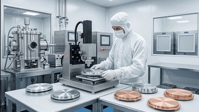
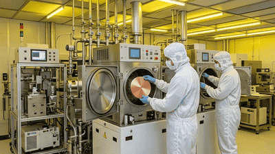
In sputtering, energetic ions strike a target and eject material that deposits onto the wafer. The target supplies the material, while the deposition equipment and operating conditions shape the resulting film.
This is a form of physical vapor deposition, commonly called PVD. Semiconductor applications include aluminum metallization, titanium-based layers, barriers, and copper seed deposition.
A target is therefore not equivalent to the finished interconnect. Between the two sit deposition, patterning, additional processing, and quality control.
That distinction matters for investment analysis. Growth in the use of a metal does not automatically produce proportional growth in sputtering targets made from that metal.
Aluminum, copper, titanium, and cobalt should not be arranged as successive generations of one interchangeable product.
Some layers carry most of the current. Others improve adhesion, restrict diffusion, or create a suitable interface for subsequent deposition.
A chip can use aluminum at a bonding interface, copper in wiring, titanium-containing films around contacts, and cobalt in selected local structures.
Different devices also adopt different metallization schemes. Mature-node analog chips, advanced logic, memory, and packaging do not share one universal transition schedule. The relevant unit of analysis is the qualified process layer, not the periodic-table symbol alone.
Aluminum’s historical importance does not disappear because advanced interconnects require other materials. Established processes and selected interface applications continue to use it.
Applied Materials lists aluminum slab and bond-pad metallization among common PVD applications. That reinforces the distinction between an advanced logic wiring transition and the broader demand for aluminum deposition.
From the factory manager’s perspective, a proven aluminum process remains valuable when it meets performance and cost requirements.
From the supplier’s perspective, the opportunity lies in dependable quality and a diverse installed base. Older technology does not necessarily mean a declining business, although its growth drivers differ from leading-edge logic.
Copper became attractive for interconnects because of its electrical properties. At larger dimensions, those properties remain compelling.
As lines become narrower, however, effective resistance rises. Surface and grain-boundary effects become more important, while supporting layers occupy a larger share of the available space.
Imec’s research emphasizes that alternative conductors can have higher resistivity than copper at larger dimensions yet become more competitive as dimensions shrink because their resistivity increases differently.
The comparison is therefore not simply which bulk metal has the lowest resistivity. It is which complete structure offers the best electrical behavior at the required dimensions.
In a conventional copper damascene flow, trenches and vias are formed in the dielectric, supporting films are deposited, and copper is introduced before excess material is removed.
PVD can provide a copper seed layer that supports subsequent electrochemical filling. The target does not necessarily supply all the copper in the completed feature.
Applied Materials identifies copper barrier and seed deposition as established PVD interconnect applications.
This distinction prevents a common forecasting error. More copper wiring does not imply that every additional unit of deposited copper comes from a sputtering target. Target demand follows the specific deposited layers and their processing requirements.
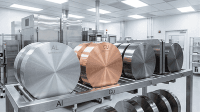
Titanium’s contribution is frequently different from copper’s. It can support adhesion, contact formation, or selected barrier-related functions depending on the process.
Titanium nitride is also important, but metallic titanium and titanium nitride are not identical products. A titanium-containing film can be formed through reactive sputtering or through other deposition approaches.
Applied Materials describes a cobalt contact flow using PVD titanium and ALD titanium nitride before subsequent cobalt deposition.
For a target supplier, the addressable opportunity depends on which layer is sputtered. A rise in titanium-nitride use does not automatically translate into the same increase in titanium target sales.
Cobalt is sometimes described as a copper replacement. In practice, it can also help copper remain usable at smaller dimensions.
A liner can influence adhesion and interface behavior while occupying space that might otherwise contain the principal conductor. Changing the liner system can improve the balance between reliability and resistance.
Applied Materials has described cobalt’s role in reducing the total thickness of supporting layers within copper interconnect structures.
That makes the transition more nuanced than one metal displacing another. Cobalt adoption can support continued copper scaling, creating complementary demand within a shared process rather than an immediate winner-takes-all substitution.
Deep, narrow structures can be difficult to fill using a directional deposition process alone. Manufacturers may combine several techniques to establish interfaces and complete the feature.
Applied Materials’ cobalt suite illustrates this division: PVD deposits an initial cobalt layer, CVD supplies fill, and additional processing addresses seams, grains, and resistance.
A cobalt target therefore represents only one part of the materials opportunity. Chemical precursors and process gases can capture value elsewhere in the same flow.
The investor must follow the deposition sequence. Counting the entire cobalt structure as target-derived material exaggerates the target supplier’s exposure.
Supporting films become proportionally more expensive in geometric terms as the feature narrows. A layer that appears thin in absolute units can occupy a substantial fraction of the cross-section.
The keyword is integration. Conductors, barriers, liners, dielectrics, and deposition methods must work together to preserve useful electrical performance.
Removing a layer can free conducting space but create an adhesion or reliability problem. Making a layer thinner can help resistance but challenge process control.
This explains why successful materials transitions are rarely isolated substitutions. They involve a coordinated change in the structure and the manufacturing sequence.
Although the title focuses on four metals, ruthenium matters because it can alter the role of cobalt and copper in advanced schemes.
Applied Materials currently describes an interconnect system using a ruthenium-cobalt liner alongside selective ALD barriers and copper reflow. The offering combines multiple processes rather than relying on a single replacement material.
That does not establish one universal future architecture. It shows that development continues beyond a fixed aluminum-to-cobalt narrative.
Target suppliers should monitor alternative metals, but also identify whether those metals enter through sputtering, chemical deposition, or a combination. Technology relevance and target-market relevance are different measurements.
A high-purity target must also perform consistently during deposition. Composition alone does not describe every relevant manufacturing characteristic.
Microstructure, inclusions, density, dimensions, surface preparation, and the target assembly can influence behavior in the tool.
Customers ultimately care about deposited-film quality and process stability. A favorable certificate cannot compensate for unacceptable particles or inconsistent operating performance.
The supplier’s advantage therefore extends beyond refining metal. It includes manufacturing control, analytical verification, traceability, and an understanding of the customer’s deposition environment.
Introducing a new target can require evaluation of the film and the wider process. Customers need confidence that repeated lots behave consistently and do not compromise device performance.
This gives qualified suppliers a defensible position. Switching can consume engineering effort and equipment time.
However, customers retain reasons to qualify alternatives, including supply resilience and purchasing leverage. New process generations can also reopen competition.
The durable supplier is not merely the incumbent. It is the company that continues to meet evolving requirements while delivering acceptable economics and dependable supply.
Target demand reflects production volume, the number of sputtered layers, deposited thickness, and material utilization.
A more complex chip may require additional deposition steps, but thinner films or process changes can offset part of that growth.
Target replacement schedules and customer inventories can also make quarterly shipments uneven.
A useful forecast separates wafer activity from deposition intensity. It then examines which layers use each metal and whether the deposition method is changing. Broad semiconductor revenue growth is too distant from these operating details to serve as a complete target-demand model.
Used targets can retain valuable material. Recovery and refining can return some of that value to the supply chain, subject to composition and quality requirements.
Commercial arrangements may account separately for metal value and manufacturing services. Those arrangements influence inventory, working capital, and reported revenue.
A rise in metal prices can therefore increase sales without an equivalent improvement in profitability.
For investors, manufacturing value added and cash conversion can be more informative than headline revenue growth. Recycling capability is valuable when it supports reliable output and sensible economics, not merely because recovered tonnage is high.
Interconnect changes influence more than targets. Photoresists help define structures. Gases and precursors support deposition and etching. Cleaning chemicals manage residues. CMP consumables remove excess material and restore planarity.
A transition toward chemical deposition can shift spending away from one target application while increasing demand for another materials category.
Even within one manufacturer, the financial beneficiaries may differ by process level.
Portfolio analysis should therefore map the complete flow. A target-focused company and a precursor supplier can both participate in advanced interconnects without having the same growth sensitivity or competitive risks.
The process engineer asks whether the complete stack meets resistance, reliability, and defect requirements.
The procurement manager asks whether qualified material can arrive consistently from a resilient supply chain.
The supplier asks whether the application requires capabilities that support attractive margins.
The investor asks whether those margins translate into cash returns after research spending, capacity investment, and working-capital needs.
Each perspective is useful. None should be replaced by a simple prediction that one metal’s adoption guarantees another company’s growth.
Evaluate the opportunity through specific questions:
These questions turn a materials-transition theme into an assessable business case.
Advanced interconnects are not abandoning older metals in one synchronized sequence. They are assigning materials more precisely to the functions each can perform.
Aluminum remains useful in established metallization. Copper continues to benefit from improved supporting layers. Titanium contributes to selected interfaces. Cobalt can support both alternative conductors and continued copper scaling.
The strongest target suppliers will combine high-quality material with process knowledge, reliable manufacturing, and disciplined economics. The opportunity lies not in guessing the next fashionable metal, but in understanding where a qualified sputtered film remains indispensable to the complete interconnect structure.